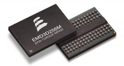
STT-MRAM is capable of high-speed operation and consumes very little power as it retains data even when the power is off. Because of these features, STT-MRAM is gaining traction as the next-generation technology for applications such as embedded memory, main memory and logic. Three large semiconductor fabrication plants have announced that risk mass-production will begin in 2018.
As memory is a vital component of computer systems, handheld devices and storage, its performance and reliability are of great importance for green energy solutions.
The current capacity of STT-MRAM is ranged between 8Mb-40Mb. But to make STT-MRAM more practical, it is necessary to increase the memory density. The team at the Center for Innovative Integrated Electronic Systems (CIES) has increased the memory density of STT-MRAM by intensively developing STT-MRAMs in which magnetic tunnel junctions (MTJs) are integrated with CMOS. This will significantly reduce the power-consumption of embedded memory such as cache and eFlash memory.
MTJs were miniaturized through a series of process developments. To reduce the memory size needed for higher-density STT-MRAM, the MTJs were formed directly on via holes - small openings that allow a conductive connection between the different layers of a semiconductor device. By using the reduced size memory cell, the research group has designed 128Mb-density STT-MRAM and fabricated a chip.
In the fabricated chip, the researchers measured a write speed of subarray. As a result, high-speed operation with 14ns was demonstrated at a low power supply voltage of 1.2 V. To date, this is the fastest write speed operation in an STT-MRAM chip with a density over 100Mb in the world.
Source https://www.ecnmag.com/news/2018/12/researchers-develop-128mb-stt-mram-worlds-fastest-write-speed-embedded-memory

